BGA (Ball Grid Array) is one type of packaging for surface-mounted integrated electronic circuits (integrated circuits whose components are actually ‘mounted’ or affixed on the surface of the printed circuit semiconductor board). A BGA package simply looks like a thin wafer of semi-conducting material that has circuit components on only one face. The Ball Grid Array package is called such because it is basically an array of metal alloy balls arranged in a grid.
Ball Grid Array versus Pin Grid Array
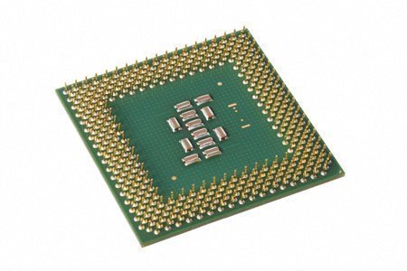
There is one other common packaging for integrated circuits and this is the PGA or Pin Grid Array. The BGA looks physically similar to a Pin Grid Array package. Both are one-sided; that is, only one face of the semi-conducting substrate is used for printing and mounting of circuit components. Moreover, both have an obvious grid-like pattern. However, the Pin Grid Array uses pins – thus, the name – whereas the BGA uses balls – as it has already been mentioned above. The pins (in the PGA) or the balls (in the BGA) are the materials through which electricity is conducted between the printed surface of the semiconductor board and the surface-mounted circuit components.
Manufacture of a Ball Grid Array Packaging
The manufacture begins with the basic circuit board, primed and printed. This printed circuit board for BGA has pads made of copper and these are arranged in the grid pattern that the solder balls are designed to have.
After the solder balls have been precisely arranged on the surface of the printed circuit board, the soldering process would begin. Surface mount soldering would proceed through reflow soldering (with the aid of a reflow oven that uses infrared or vapors as the heat source). At this point, the metal alloy balls would melt due to extreme temperatures. As the whole assembly cools, the solder balls will solidify and the package will become firmly affixed to the circuit board.
The Advantages of Ball Grid Array
A Ball Grid Array makes precise alignment and mounting possible. Before the Ball grid Array packaging, a single circuit board would sometimes require hundreds of pins. This presented a lot of positioning problems. When the assembly was heated, adjacent pins would sometimes get soldered together or form unplanned bridges.
One other advantage of Ball Grid Array packaging over other types of packaging involves heat conduction. A Ball Grid Array has less resistance to heat so heat flows readily from the mounted circuit components to the printed circuit board. This reduces the risk of overheating.
Finally, a Ball Grid Array assembly’s contact points (point of contact between the surface solder balls and the printed circuit board itself is not readily apparent. This means greater data and application security.
Of course, a Ball Grid Array packaged integrated circuit is rather inflexible. Rigorous stress on the integrated circuit may cause the balls or the contact points to break off. Furthermore, if flaws in design or construction need to be found, expensive tools would be needed.


Follow Us!